
Development Status of Compound Semiconductor Cutting, Grinding, and Polishing Equipment
Overview of Compound Semiconductor Development
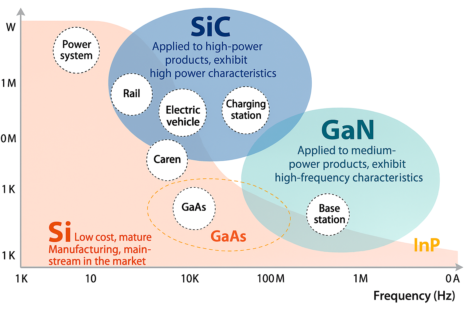
Most common semiconductor-related products (such as mobile phone chips) are primarily made from first-class semiconductor material—silicon (Si). However, as technology advances, market demands for higher specifications have increased. Silicon-based semiconductors are gradually approaching their physical limits, driving the emergence of new semiconductor materials. These materials are compounds composed of two or more elements, including second-class semiconductor materials like gallium arsenide (GaAs) and indium phosphide (InP), as well as third-class semiconductor materials—silicon carbide (SiC) and gallium nitride (GaN), collectively referred to here as compound semiconductors.
Compared with traditional silicon-based and III-V group semiconductors, SiC and GaN operate more stably under high temperature, high pressure, and high current conditions. They can be applied to high-power, high-switching-frequency products and offer superior heat dissipation. With the rise of 5G, electric vehicles, and growing global emphasis on carbon reduction, the development of energy-efficient, low-power compound semiconductors has accelerated.
 |
Source: Infineon, Digitimes / Compiled by Metal Industries Research & Development Centre (MII)
Summary of Compound Semiconductor Processing
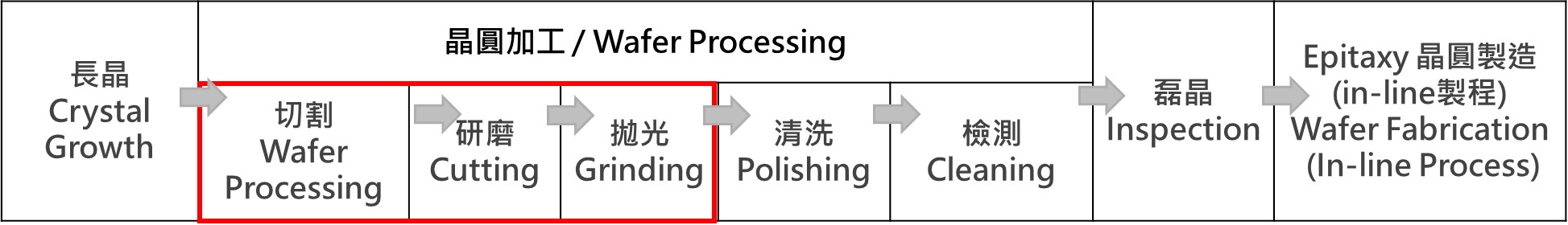
According to Yole, the global SiC wafer market reached $2.7 billion in 2023 and is expected to grow to $10.4 billion by 2029, driven by automotive applications, with a CAGR of 25%. To meet the manufacturing needs of high-performance chips, high-quality SiC wafer substrates are required. These substrates are produced after SiC crystal growth and subsequent processing steps, which include cutting, grinding, polishing, cleaning, and inspection. After wafer fabrication, an epitaxial process deposits a high-quality crystalline layer on the wafer surface to enhance chip performance.
However, SiC’s hardness—second only to diamond and boron carbide (B4C)—makes processing extremely challenging. Its brittleness and low fracture toughness lead to brittle fractures during machining, leaving damaged layers or severe surface/subsurface defects that affect precision. Below is a detailed explanation of the critical cutting, grinding, and polishing processes.
 |
Source: Compiled by Metal Industries Research & Development Centre (MII)
Cutting
Diamond Wire Cutting
Currently the mainstream SiC wafer slicing technology, diamond wire cutting uses blades slightly harder than SiC. The process is time-consuming—about 2.4 hours per wafer and over 48 hours for an entire ingot—with significant material loss (equal to wire diameter, 80–150 μm) and frequent tool wear. However, it supports batch production.
Laser Cutting
Laser cutting uses high-energy beams to locally melt or vaporize material for wafer separation. It includes full-cut, half-cut, and stealth dicing. Full-cut is non-contact, avoiding mechanical stress and tool wear, while stealth dicing modifies material internally and then applies stress for separation. Laser cutting reduces slicing time by 85% and material loss by 70% compared to diamond wire cutting, though technology is dominated by foreign firms.
Grinding and Polishing
After cutting, SiC wafers are rough and uneven, requiring grinding, lapping, and polishing. Due to SiC’s hardness and chemical resistance, these steps are time-intensive. Chemical conditions (slurry composition, concentration) and mechanical factors (particle size, pad structure) significantly affect results. Polishing typically uses Chemical-Mechanical Polishing (CMP) with highly oxidative slurry, which shortens equipment life and raises water and disposal costs.
Global Equipment Manufacturers
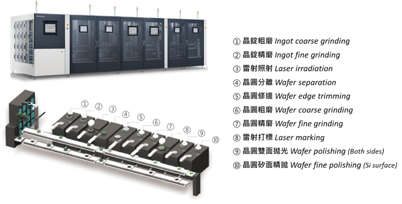
Disco (Japan)
Disco specializes in semiconductor grinding and cutting, holding 78.8% of SiC cutting and 57.1% of grinding equipment market share in 2023. Its KABRA technology (2016) uses laser irradiation to form a separation layer, reducing processing time and material loss. Compared to traditional methods (100 hours for 32 wafers), KABRA produces 46 wafers in 31 hours. The KABRA! Zen system integrates 10 steps in one machine for 8-inch wafers. In 2023, Disco launched DDS2020 with Stealth dicing™, boosting cutting speed 10x. Disco plans to triple production capacity in 10 years, investing ¥80 billion in new plants.
Tokyo Seimitsu (Accretech, Japan)
Ranked second globally, Tokyo Seimitsu offers high-rigidity grinders for hard materials. Models like HRG200X grind SiC wafers to 120 μm in one minute, while HRG300 series supports 8/12-inch wafers with high precision (TTV < 0.5 μm). The HRG3000RMX model is expanding in Europe, the U.S., and China.
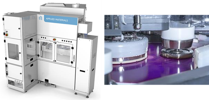
Applied Materials (USA)
A global top-five semiconductor equipment supplier, Applied Materials dominates CMP systems. In 2021, it introduced the Mirra® Durum™ CMP system for 8-inch SiC wafers, integrating polishing, measurement, cleaning, and drying for automated dry-in/dry-out processing. It reduces surface roughness 50x compared to grinding and 3x compared to batch CMP.
 |
Source: Disco, Compiled by Metal Industries Research & Development Centre (MII)
圖4 Mirra® Durum™ CMP系統
 |
Source: Applied Materials, Compiled by Metal Industries Research & Development Centre (MII)
Conclusion – Opportunities for Machine Tool Manufacturers
While silicon-based semiconductor demand has fluctuated, SiC-related equipment demand continues to grow. SiC’s hardness and brittleness pose challenges, creating high entry barriers dominated by a few global players. Taiwanese machine tool manufacturers—experts in cutting, grinding, and polishing—could upgrade existing tools to address SiC processing pain points and enter the semiconductor equipment market after wafer fab validation. Studying leading firms’ technology gaps and securing beta-site verification will help develop market-ready solutions and open export opportunities.


