

Beyond the Chip: Machine Tool Opportunities in Advanced Packaging at SEMICON 2026
Viewed as a whole, SEMICON Taiwan 2026 delivered one particularly clear industry signal: advanced packaging is rapidly becoming a critical enabler of semiconductor innovation at the system level.
A review of the exhibition themes over the past three years clearly shows a shift in the industry’s technical focus. In 2024, “Breaking Limits: Powering the AI Era” brought AI, advanced processes, and advanced packaging into the same industry roadmap. In 2025, the emphasis moved further toward collaboration and heterogeneous integration. By 2026, the focus had evolved to system-level innovation. The most representative change this year was the transition from pursuing the scaling and performance of individual chips to integrating different chips, materials, and processes to improve overall AI-system performance. [1][2][3]
What the Exhibition Revealed: Advanced Packaging and Problem-Solving Solutions Take Center Stage
The overall floorplan and exhibitor displays highlighted several notable changes: technologies related to advanced packaging were significantly more visible; problem-solving solutions stood out more prominently; and industry discussion increasingly shifted from the performance of individual machines toward process integration and system-level innovation. Across Nangang Exhibition Halls 1 and 2, two clear phenomena emerged.
First, complete displays of large front-end or midstream process equipment were relatively limited, while bonding, grinding, dicing, inspection, metrology, and advanced packaging equipment for 3DIC, FOPLP, and chiplets were much more visible. This does not mean that front-end or midstream processes have become less important; rather, packaging, testing, metrology, and automation enjoyed particularly high visibility this year. SEMI’s post-show data also indicated that nearly 300 companies participated in the 2026 Packaging Technology Concept Area, up 6% year on year, making it one of the exhibition’s two fastest-growing areas. [4]
Second, collaboration across the industrial ecosystem has become increasingly evident. In 2025, SEMI established the 3DIC Advanced Manufacturing Alliance to connect wafer manufacturers, OSAT providers, equipment suppliers, and materials companies. This year, many exhibitors appeared as alliances, corporate groups, or cross-domain partnerships, revealing that the semiconductor supply chain is moving toward tighter integration. Hermes-Epitek exhibited process, materials, and testing solutions together with affiliated companies and partners [5]; the G2C+ alliance, formed by C SUN, GPM, and GP, promoted a one-stop solution [6]; Gudeng extended its carrier expertise into automation, cleaning, and AOI partnerships [7]; and Grand Process Technology expanded from wet-process equipment into materials and industry–academia collaboration [8]. These examples show that competition is no longer based solely on the performance of a single machine, but also on the ability to integrate different areas of expertise and provide more complete solutions to process pain points.
Another noteworthy feature was that many companies no longer presented only equipment specifications and performance parameters. Instead, they directly addressed process bottlenecks with integrated solutions. As panel-level packaging grows in size, for example, equipment suppliers are proposing combined solutions for warpage control, thermal management, dispensing, and large-format handling; materials suppliers are likewise incorporating low-stress design, warpage management, and reliability validation into their overall approaches. [9][10] The semiconductor industry is inherently process-intensive and highly integrated. For machine tool companies, the key lesson is to begin with the customer’s process problem. The industry has traditionally started from machine specifications, accuracy, spindle speed, or travel. To enter different end-use sectors, however, it must first understand customer pain points and then combine machining, spindle, motion, metrology, and automation capabilities into implementable solutions.
The Era of Large-Format Packaging Has Arrived
“The era of large-format packaging” is not an official exhibition term, but an industry phenomenon inferred from the content presented at SEMICON Taiwan 2026. Beyond front-end and midstream processes, a large share of the most visible technologies, equipment, and peripheral solutions revolved directly or indirectly around advanced packaging, testing, materials, inspection, and automation. This reflects the growing role of advanced packaging as a key enabler of AI innovation at the system level. Different AI applications impose different requirements for computing power, memory, bandwidth, power consumption, and cost. IC design companies are therefore developing architectures such as GPUs and ASICs while integrating HBM, I/O dies, and chiplets with different functions. SEMI has likewise noted that AI competition is moving beyond the performance of individual chips toward system-level integration, with HBM and high-speed optical interconnects becoming critical. [11][12]
When a single die can no longer simultaneously satisfy requirements for computing power, bandwidth, heat dissipation, and cost, heterogeneous integration becomes as important as advanced process nodes. This is why 2.5D, 3D, CoWoS, FOPLP, CoPoS, glass-core substrates, hybrid bonding, and co-packaged optics (CPO) are attracting rapid attention. SEMICON 2026 introduced its first Chiplet Pavilion, directly reflecting the demand from AI and HPC for heterogeneous integration and high-precision packaging equipment. [3]
For the machine tool industry, the key is not to predict which single technology will prevail, but to recognize that no single path has yet become definitive. Different AI architectures, HBM configurations, package sizes, power requirements, and thermal conditions may call for different packaging solutions. As long as packaging architectures continue to evolve, requirements for materials, dimensions, carriers, machining, handling, positioning, metrology, and equipment will evolve with them. The opportunity in advanced packaging therefore comes not only from market growth, but also from the fact that new processes and equipment requirements are still taking shape.
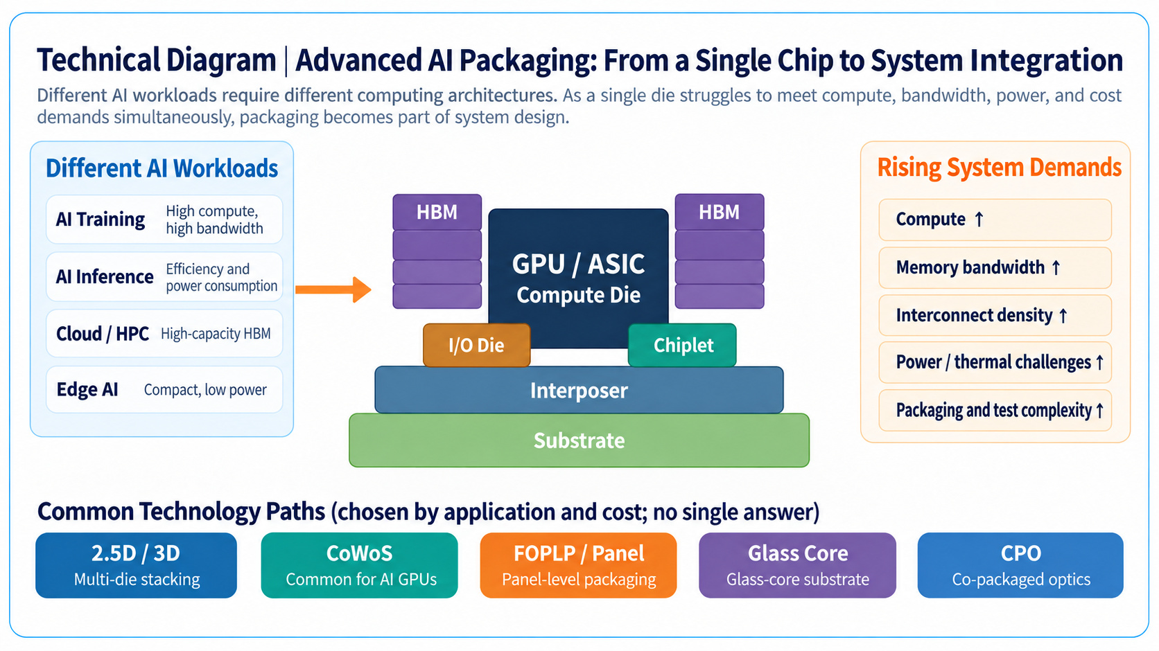 |
Source:TMBA (2026)
|
Note: This is a conceptual technical illustration, not an actual machine or a product from a specific supplier. Different AI workloads have different requirements for computing power, memory bandwidth, power consumption, and cost. GPUs/ASICs, HBM, I/O dies, and chiplets may therefore be integrated through 2.5D/3D, CoWoS, and other approaches. The point is not that one packaging technology will necessarily prevail, but that system design and packaging jointly determine performance. |
Another important development is the increasing convergence of back-end packaging requirements with front-end process standards. This does not mean that packaging is literally becoming wafer front-end processing; rather, the requirements for accuracy, flatness, thickness control, cleanliness, micro-hole fabrication, positioning, and metrology continue to rise. Translated into terms familiar to the machine tool industry, the equipment requirements visible at the show can be summarized as six capabilities: grinding, thinning, planarization, hole-making, precision, and cleanliness. “Grinding” covers grinding, polishing, CMP, and surface-quality control. “Thinning” refers to reducing and controlling the thickness of chips, substrates, or carriers to enable stacking and shorten interconnect paths. “Planarization” concerns flatness, thickness uniformity, and warpage control. “Hole-making” includes microvias, through-holes, and related processes required for high-density interconnects. “Precision” denotes the positioning accuracy, repeatability, and metrology demanded by packaging, testing, and CPO alignment. “Cleanliness” corresponds to the clean environments, contamination control, and process stability required for advanced packaging. These six capabilities are not merely slogans; they describe the concrete ways in which advanced packaging is driving advances in precision machining, motion control, metrology, structural stability, and automation—and they point to areas where the machine tool industry can participate.
“Precision Manufacturing Stands Behind Every Chip” — Another Opportunity for Machine Tools
This echoes the slogan adopted by TMBA for its SEMICON Taiwan delegation this year: “Precision Manufacturing Stands Behind Every Chip.” The TMBA SMART TEAM brought together capabilities in precision machining, spindles, grinding, mineral casting, temperature control, and equipment validation to connect the machine tool supply chain with semiconductor-equipment demand. [13] Machine tools may not machine chips directly, but opportunities often lie in semiconductor equipment, precision components, and special-purpose machines created for new processes.
Grinding is one example. Grinding machines were among the first categories of machine tools to find applications in semiconductor manufacturing, from silicon-ingot and wafer grinding to wafer back grinding and thinning. DISCO’s public technical information shows that wafer thinning, ultra-thin grinding, and processes related to 3D stacking rely heavily on grinding and polishing. Recent equipment places even greater emphasis on low total thickness variation (TTV), cleanliness, and high-precision thinning. [14][15] In the era of large-format packaging, glass, ceramics, panels, substrates, molding compounds, and composite structures may all create new requirements for grinding, polishing, and planarization beyond the wafer itself. They also impose higher demands for low TTV, minimal subsurface damage, warpage control, and the integration of metrology, thermal management, cleaning, and automation. For grinding-machine builders, the next step is not merely to extend existing wafer-thinning applications, but to identify the new materials, dimensions, and surfaces that advanced packaging will require.
Glass is another material that warrants attention. Intel states that glass substrates offer superior flatness as well as thermal and mechanical stability, supporting high-density interconnects and large advanced packages. [16] Through-glass vias (TGVs) are not necessarily produced by conventional drilling, but high-volume glass production still creates requirements for cutting, chamfering, grinding, polishing, microvia formation, handling, vacuum holding, and metrology. The challenge lies not only in technical feasibility, but also in achieving low breakage, minimal edge chipping, high flatness, and high positioning accuracy under mass-production conditions. This will place new demands on brittle-material machining, spindles, fixtures, stages, and automation.
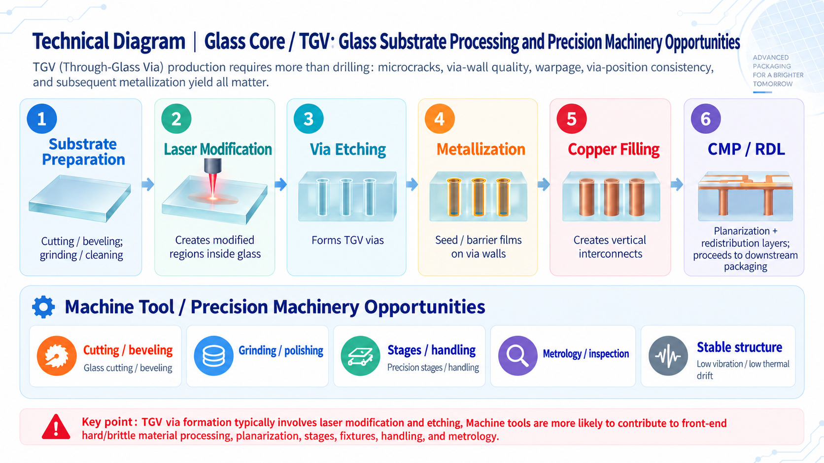 |
Source:TMBA (2026)
|
Note: This is a conceptual technical illustration, not an actual machine or a product from a specific supplier. Typical TGV process routes may include laser modification, via formation by etching, metallization, copper filling, CMP planarization, and subsequent RDL processes; actual flows vary by material and supplier. For the machine tool industry, cutting, grinding, polishing, handling, vacuum holding, precision stages, and metrology are all extendable capabilities. |
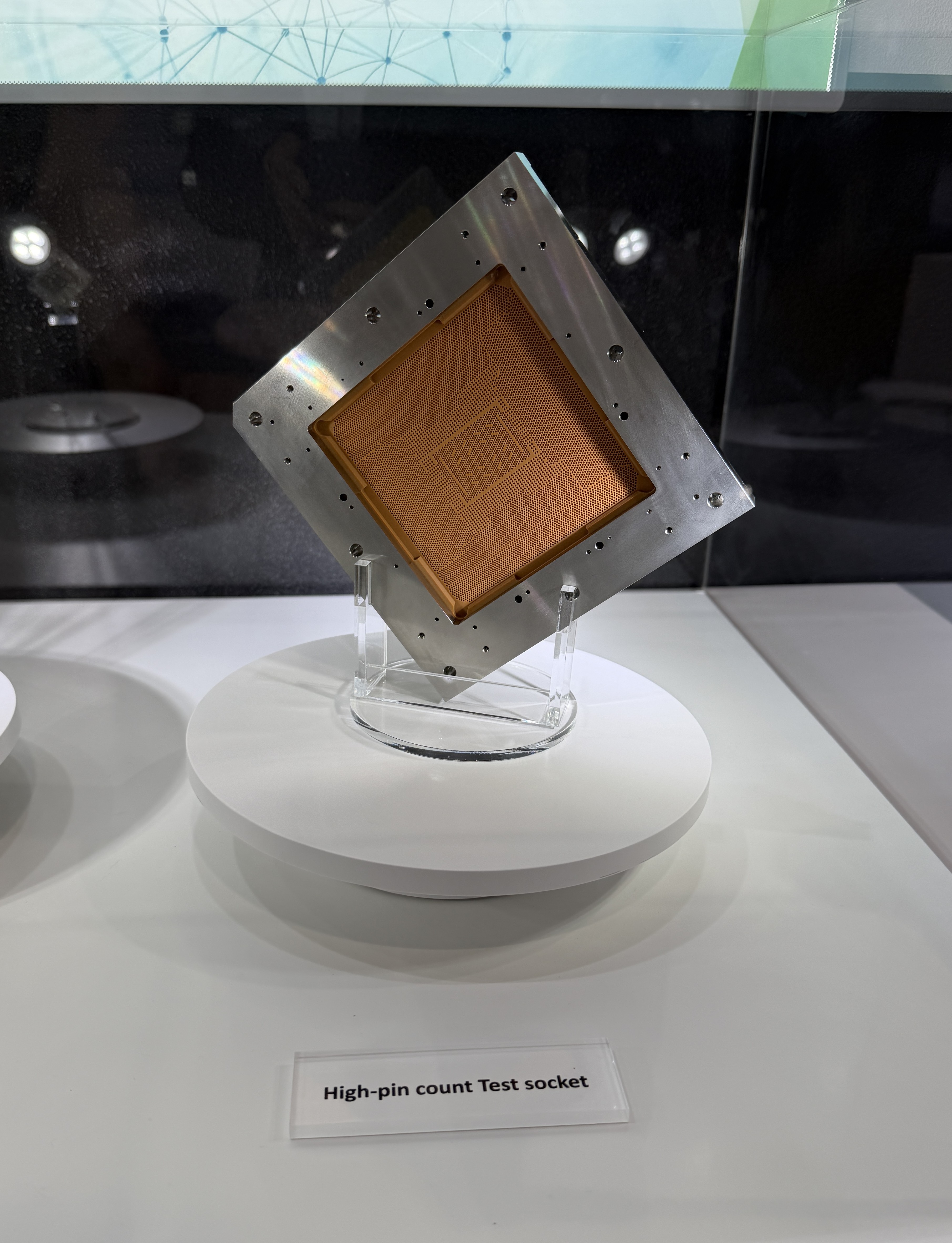
Probe cards offer similar opportunities. In addition to probes and PCBs, they contain mechanical structures such as housings, stiffeners, guide plates, and space transformers. Metal frames and reinforcement components require precision machining, while ceramic components may require micro-hole machining and grinding. Technoprobe states that housings require micron-level hole-position and flatness accuracy, while space transformers may contain hundreds or thousands of micro-holes produced with dedicated drilling equipment. [17] Precision metal parts familiar to the machine tool industry can also be found around final testing for advanced packages, including test-socket housings, frames, clamping mechanisms, thermal-management structures, and fixtures. A socket normally combines metal, engineering plastics, insulating materials, and contacts, so it should not be reduced to a single metal component. Nevertheless, Smiths Interconnect’s high-speed test socket uses a precision-machined insulated metal housing, confirming demand for precision metal machining in high-frequency, high-pin-count AI/HPC test interfaces. [18] Even highly semiconductor-specific products therefore contain potential entry points involving metal cutting, micro-hole machining, grinding, fixtures, and thermal-management structures.
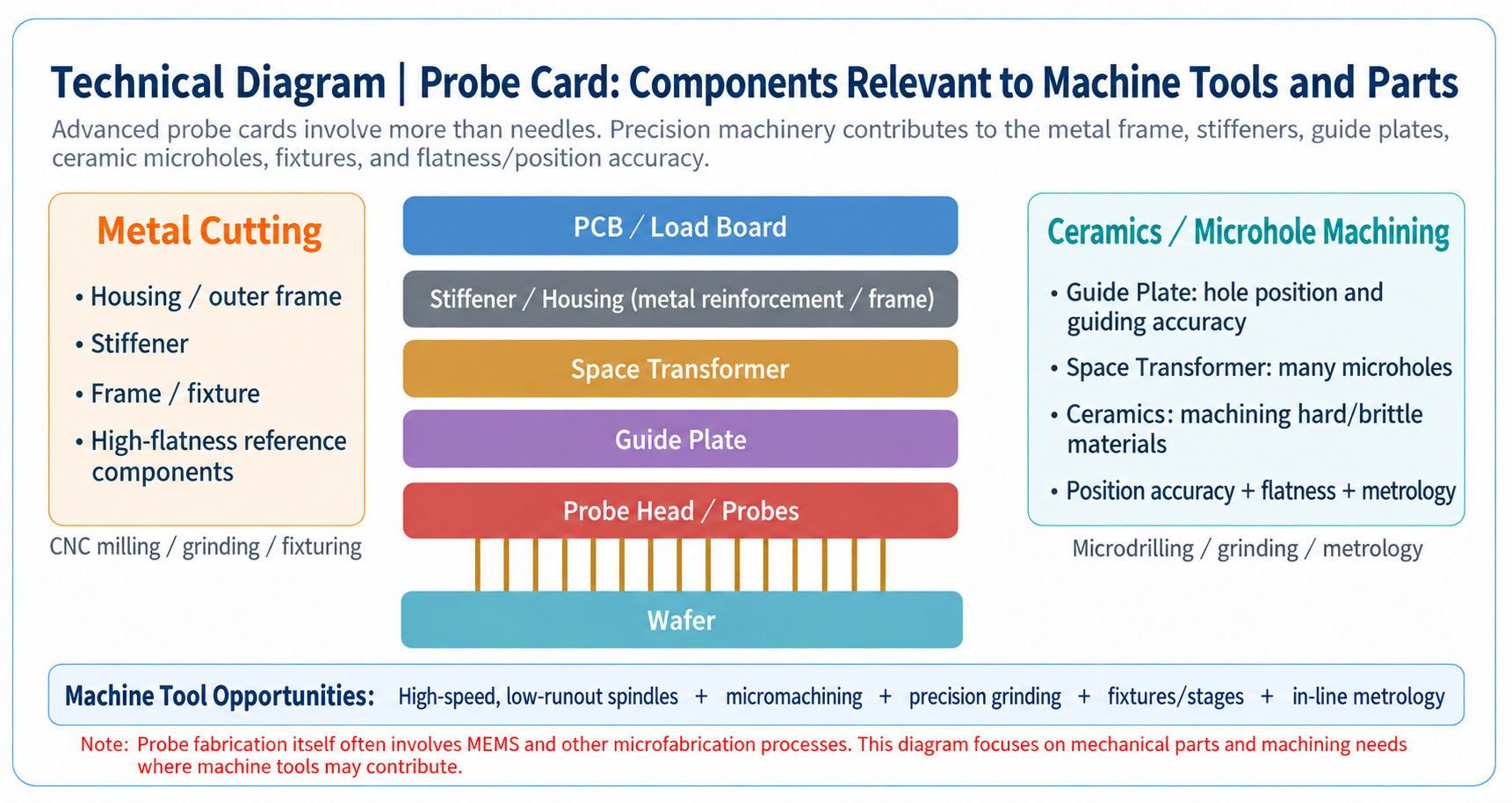 |
Source:TMBA (2026)
|
What the Exhibits Showed: What Machining Opportunities Does Advanced Packaging Create?
In addition to process equipment, physical workpieces displayed at the show gave a direct view of machining demand around advanced packaging. Probe cards and sockets involve metal frames, reinforcement, fastening, thermal structures, and fixtures. Square panels and various carriers create challenges involving large dimensions, thin plates, flatness, vacuum holding, and handling. Testing and metrology equipment directly reflect requirements for high rigidity, low vibration, and precision motion.
(The following photographs were taken at this exhibition. Many booths and machines did not permit photography because of confidentiality, customer requirements, or technologies not yet publicly disclosed. All exhibition photographs used in this article were taken with the exhibitors’ on-site consent.)
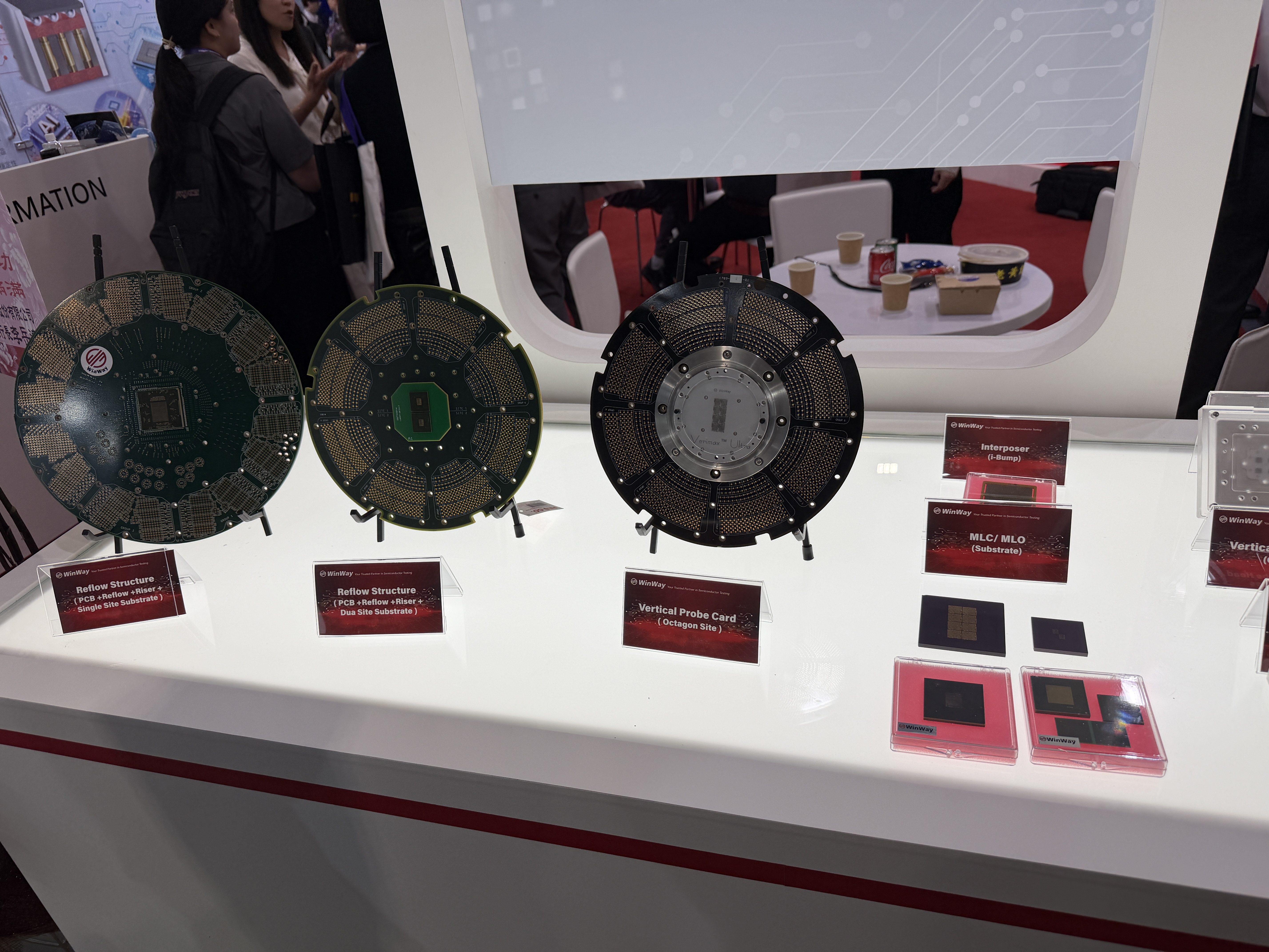 |
| Beyond the probes and PCB, the exhibit shows metal frames, reinforcement parts, fasteners, and other mechanical components, creating practical requirements for CNC milling, grinding, hole-position accuracy, and flatness control. |
 |
| The frame, fastening structure, heat-dissipation components, and fixtures often require precision metal machining. As pin counts and package areas increase, hole-position accuracy, flatness, rigidity, and repeatable clamping become more important. |
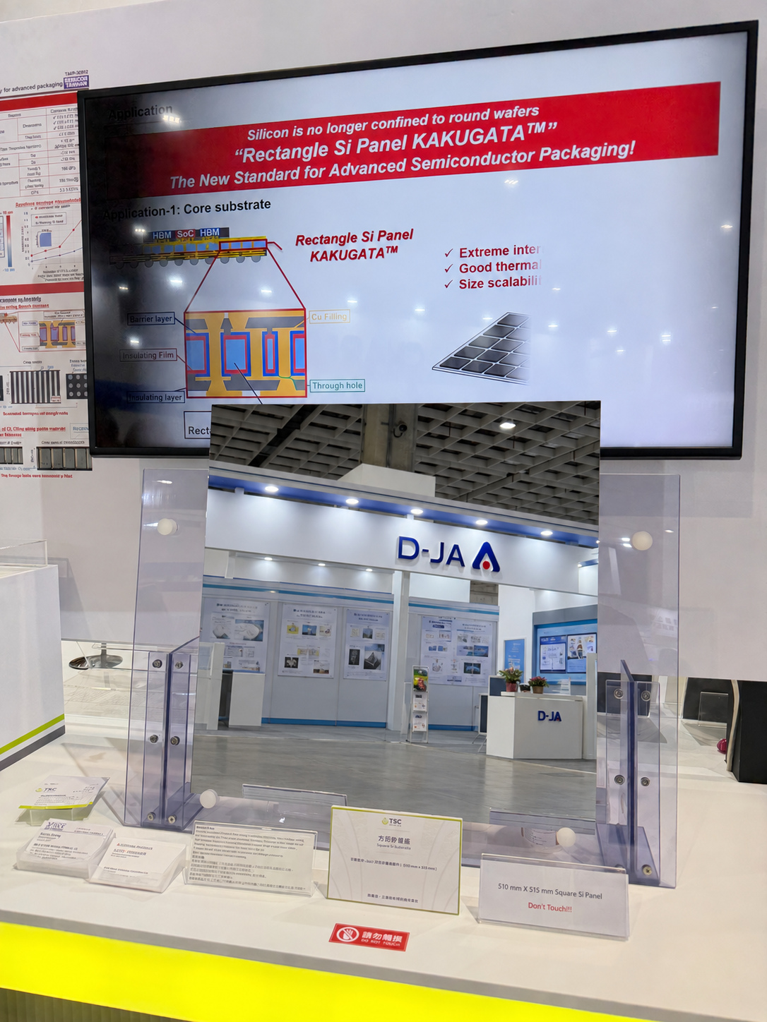 |
| The square panel illustrates the move toward larger advanced-packaging carriers. This creates challenges in flatness, warpage, vacuum holding, handling, positioning, and long-travel stages, all of which require coordinated mechanical design, motion control, and metrology. |
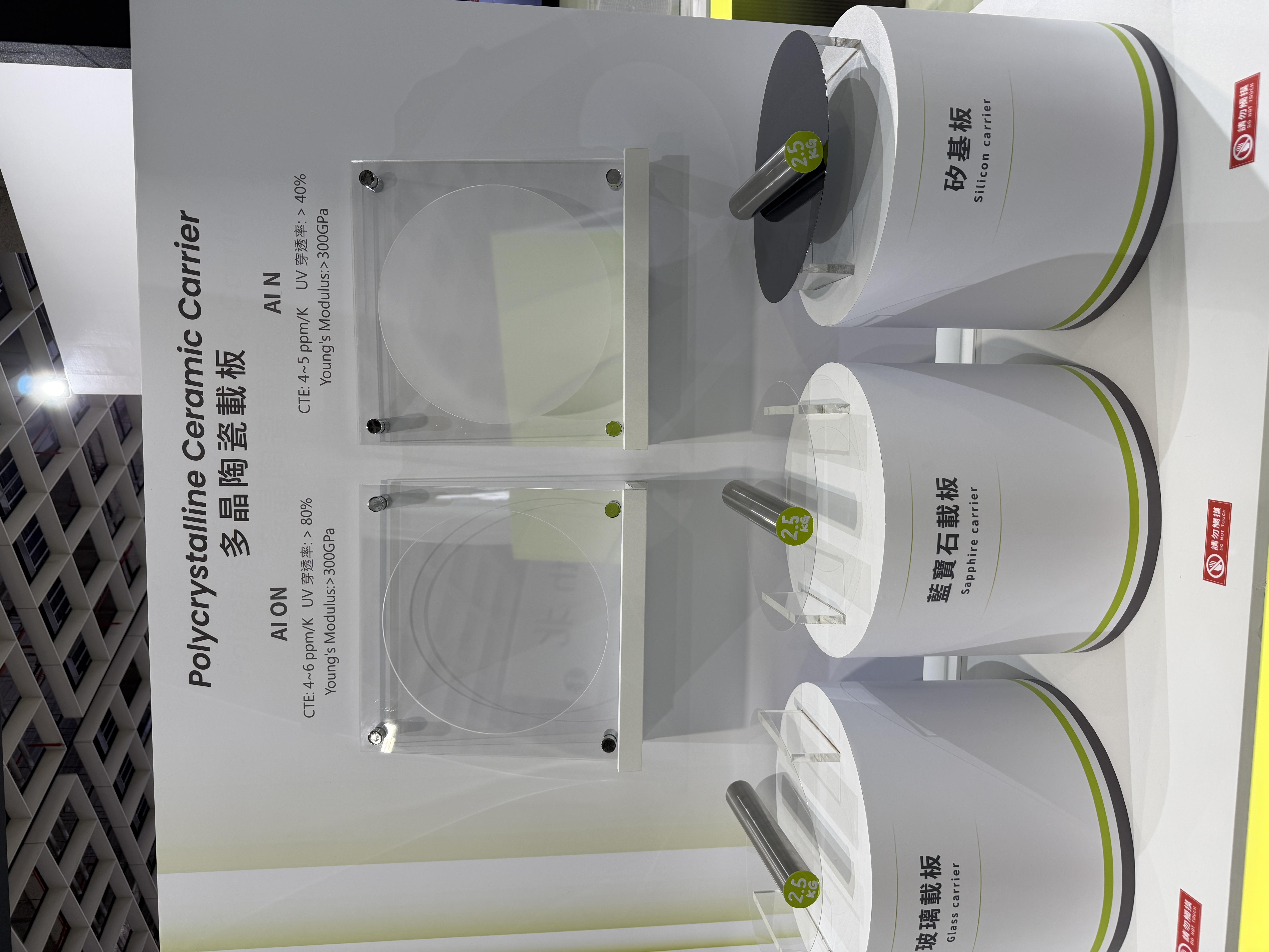 |
| The growing diversity of substrate and carrier materials means that cutting, grinding, polishing, chamfering, vacuum holding, and handling methods must be redesigned, increasing the importance of brittle-material processing, fixtures, and process control. |
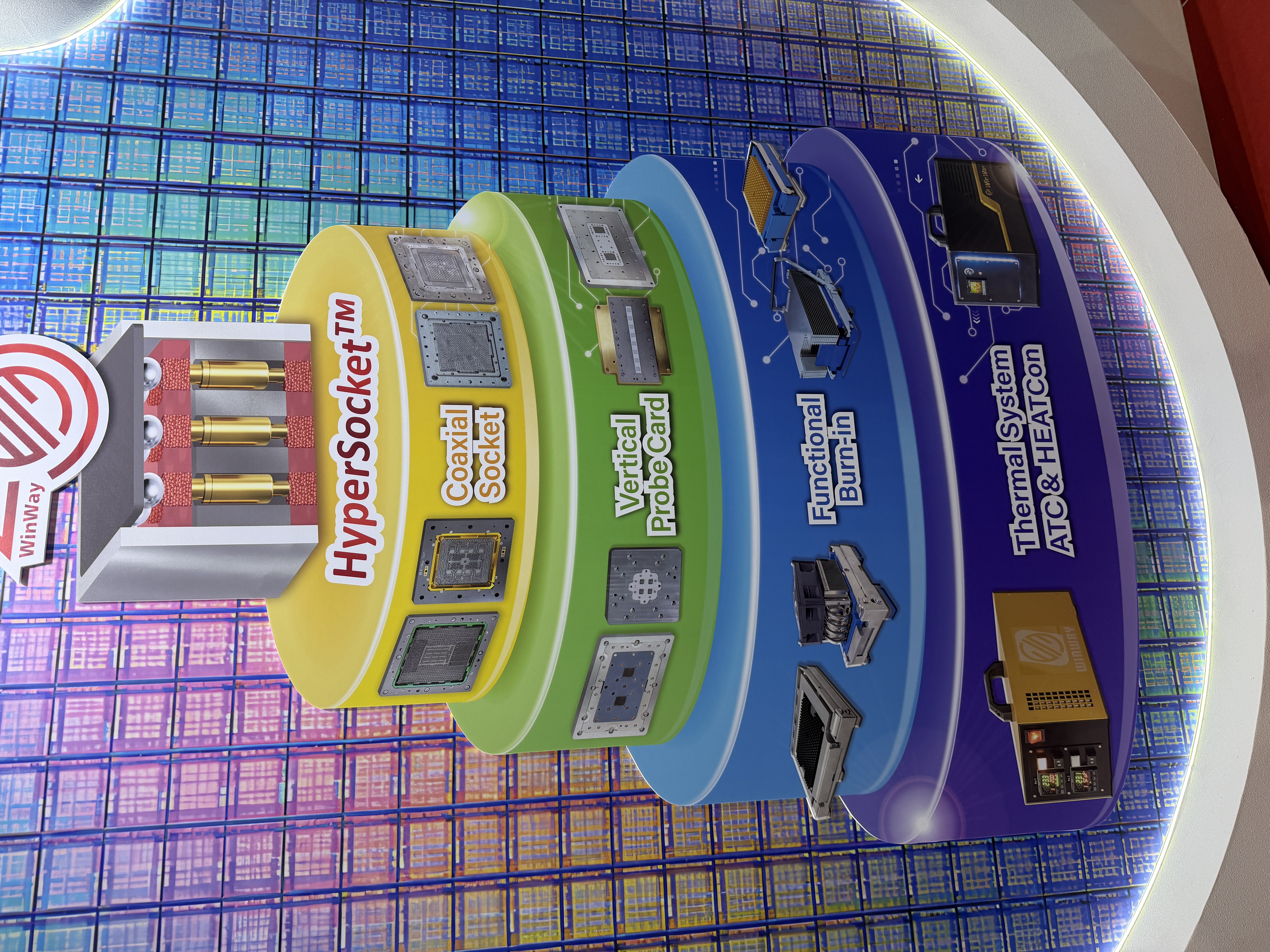 |
| As advanced packaging becomes more complex, test interfaces, fixtures, heat dissipation, clamping, and automation peripherals expand accordingly. From a machine tool perspective, this means more demand for precision parts, frames, fasteners, and modular mechanisms. |
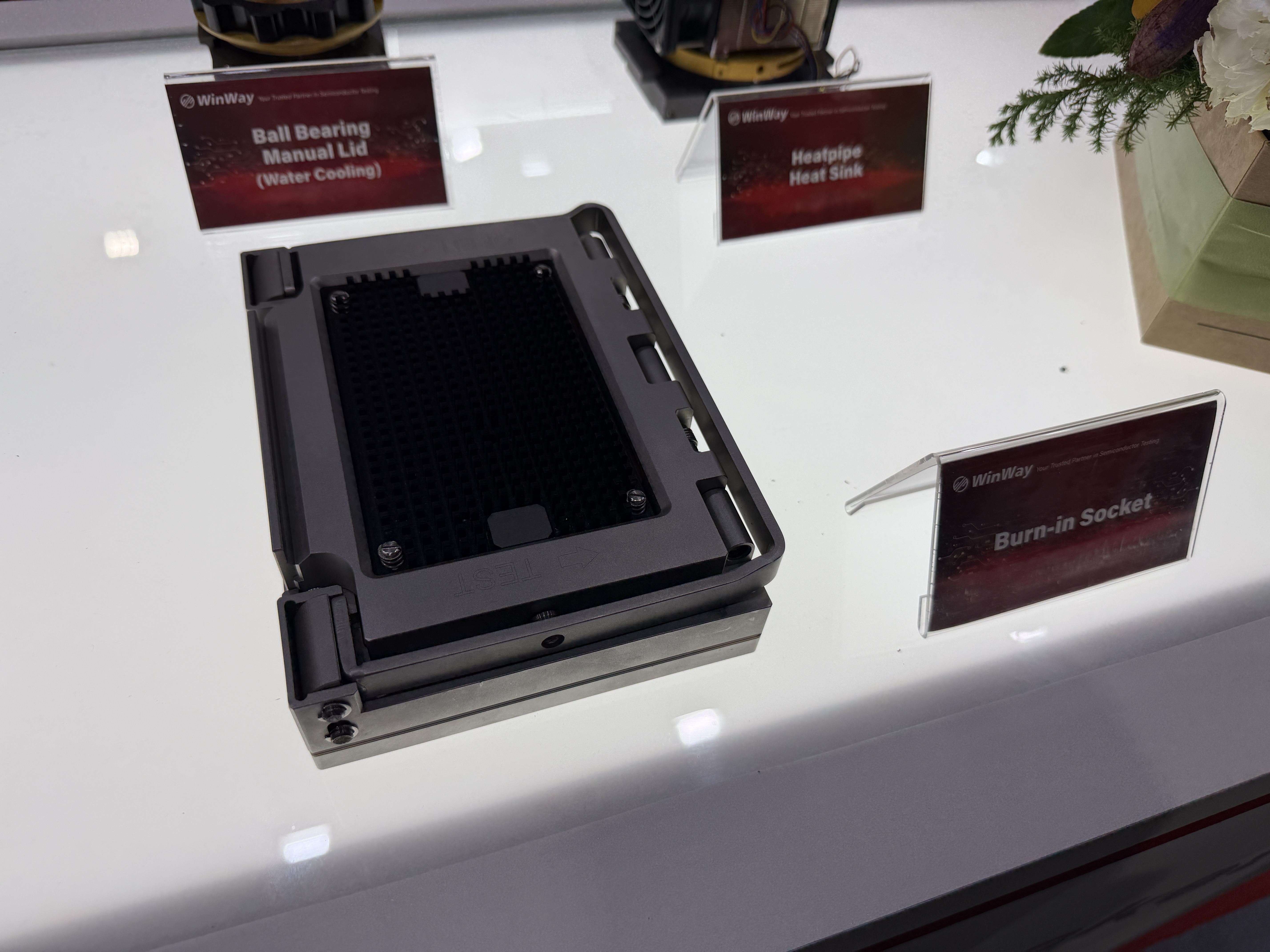 |
| Metal frames, guides, fastening features, and heat-dissipation structures are clearly visible. Such test fixtures are not machine tools, but they are workpieces that the machine tool industry can readily understand and address through precision metal cutting and mechanical design. |
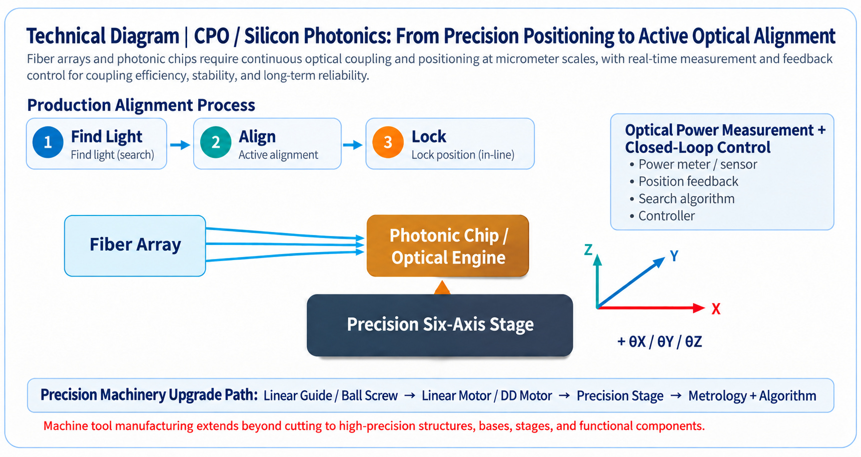
CPO and silicon photonics raise the machine tool industry’s concept of “precision” to an even higher level. Equipment requirements have progressed from linear guides and ball screws to linear motors, direct-drive motors, precision stages, and six-axis alignment; in some cases, light must remain active while the system searches, aligns, and fixes the optical path. PI’s published specifications for photonics-alignment platforms include six degrees of freedom and nanometer-level resolution, showing that speed, accuracy, and stability are now simultaneous requirements. [19] The machine tool industry’s core capabilities are not limited to cutting; they also include precision motion control. Although metal cutting and optical alignment are different applications, both extend the same underlying capabilities in mechanics, motion, and control.
 |
Source:TMBA (2026)
| Note: This is a conceptual technical illustration, not an actual machine or a product from a specific supplier. In volume production, fiber arrays and PICs/optical engines often require optical-power measurement with the light on while position is continuously corrected through a “search, align, and lock” sequence. The equipment therefore needs not only a precision stage, but also six-axis motion, closed-loop metrology, low vibration, and high repeatability. |
|
|
High precision first requires high stability. Many packaging, inspection, and positioning systems use granite or other highly stable bases because vibration, thermal drift, and structural stability directly affect process results. High-damping structural materials such as mineral casting also deserve attention. RAMPF’s public application cases include mineral-cast beds for die bonders, flip-chip bonders, and wafer saws. [20] The point is not to claim that one material is absolutely superior, but to recognize that semiconductor-equipment structures must now combine high precision with high stability rather than merely provide sufficient rigidity.
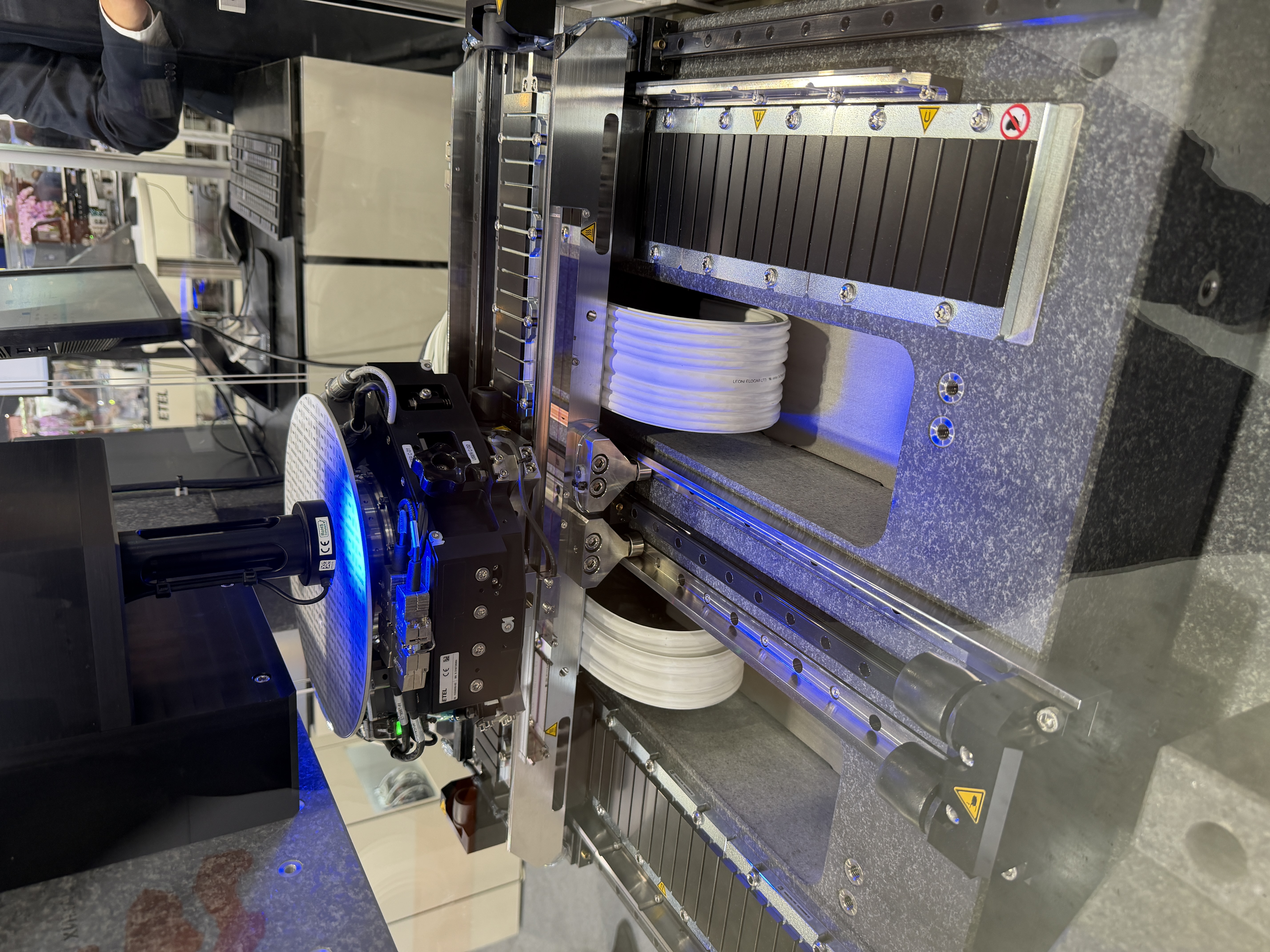 |
| As packaging, testing, and optical alignment progress to micron, sub-micron, and even nanometer levels, stability becomes the prerequisite for precision. Low vibration, high rigidity, thermal stability, and long-term geometric accuracy become central to equipment design, making granite, mineral casting, and other highly stable bases increasingly relevant to the machine tool industry. |
As Packaging Continues to Evolve, Opportunities Remain for the Machine Tool Industry
The technology trends presented at SEMICON Taiwan this year do not imply that “the semiconductor market is growing, so the machine tool industry should immediately pivot to semiconductors.” Rather, advanced packaging remains in a phase of rapid evolution. From wafers to panels, from silicon to glass, and from copper interconnects to CPO, every change in packaging architecture and materials generates new requirements for machining, handling, metrology, positioning, structures, and automation. As long as processes are still being formed and equipment specifications are not yet fully standardized, opportunities remain for the machine tool industry to participate.
The industry can consider four directions. First, companies seeking to enter the semiconductor supply chain must act more proactively by engaging with exhibitions, equipment makers, and process supply chains instead of passively waiting for semiconductor customers to issue specifications. Second, companies must understand semiconductor processes and technology trends before they can identify where their products and capabilities fit; they should also begin with end-user pain points and move from selling specifications to proposing solutions. Third, the industry should not wait until new technologies mature before preparing, but should strengthen capabilities in accuracy, reliability, cleanliness, new-material processing, metrology, and control in advance. Fourth, research institutes can help the industry develop dedicated machines and components for glass and brittle-material processing, micro-machining of advanced-packaging parts, ultra-precision grinding/thinning equipment, aerostatic spindles, and precision motion stages, while also establishing validation environments.
Taiwan’s machine tool industry has built its core strengths on machining metal quickly and precisely. To meet the emerging demands of advanced packaging and system-level integration, these capabilities can be extended into higher-value applications, including low-damage glass processing, high-flatness grinding of packaging components, highly stable precision-stage control, and support for optical-alignment equipment. This is not a departure from the machine tool industry’s core business; rather, it extends decades of accumulated precision-manufacturing expertise into the new domains of advanced semiconductor packaging and system-level innovation.
*Illustration note: The technical figures in this article are conceptual illustrations compiled from public information to help machine tool industry readers understand the relationship between processes and equipment. They do not represent actual product structures, dimensions, or any single supplier’s process flow.
References
- [1] SEMI | SEMICON Taiwan 2024: Breaking Limits: Powering the AI Era
- [2] SEMI | SEMICON Taiwan 2025: Leading with Collaboration. Innovating with the World.
- [3] SEMI | SEMICON Taiwan 2026: Smart Manufacturing and Advanced Packaging Emerge as Key Growth Areas
- [4] SEMI | SEMICON Taiwan 2026 post-show report: Nearly 300 exhibitors in the Packaging Technology Concept Area, up 6% year on year
- [5] Hermes-Epitek | “Hermes-Epitek Showcases Key Semiconductor Equipment and Quantum Technologies at SEMICON Taiwan 2026,” August 10, 2026.
- [6] G2C+ Alliance | Official “About G2C+” information.
- [7] Gudeng Precision | “Gudeng Leads Advanced Process and CoWoS Solutions.”
- [8] Grand Process Technology | Official website; “Grand Process Technology and NTUST Build an Advanced Semiconductor Packaging Talent Incubator,” January 27, 2026.
- [9] Nordson ASYMTEK | Vantage XL: Warpage control, thermal management, and large-format process integration for panel-level packaging.
- [10] Dow | SEMICON Taiwan 2026 Advanced Packaging Solutions: Materials, low stress, warpage management, and application validation.
- [11] SEMI | SEMICON Taiwan 2026: Chiplet Pavilion and AI/HPC system-level integration.
- [12] SEMI | AI Power Constraints Drive System-Level Integration: HBM, silicon photonics, and CPO.
- [13] TMBA | SEMICON Taiwan 2026 SMART TEAM: “Precision Manufacturing Stands Behind Every Chip.”
- [14] DISCO | Ultra-Thin Grinding: Ultra-thin wafer grinding and thinning.
- [15] DISCO | DFG8560 / DFG8541: Wafer thinning, TTV, and high-cleanliness grinding.
- [16] Intel | Glass Substrates for Advanced Packaging: Flatness and thermal and mechanical stability.
- [17] Technoprobe | Mechanics at Technoprobe: Housings, space transformers, and micro-hole machining.
- [18] Smiths Interconnect | DaVinci Test Socket: Precision-machined insulated metal housing for high-speed AI/HPC testing.
- [19] PI | Active Photonics Alignment: Six-axis optical alignment and nanometer-level precision motion.
- [20] RAMPF | EPUMENT Mineral Casting: Applications in die bonders, flip-chip bonders, and wafer saws.


